The winners of the annual (MC)2 image contest have been selected. We thank all the lab users who submitted and hope to feature some of the other images in various forms in the future.
Best SEM
Michal Sawczyk, “Dynamic Superchiral Particles,” acquired on the FEI Helios 650 Nanolab
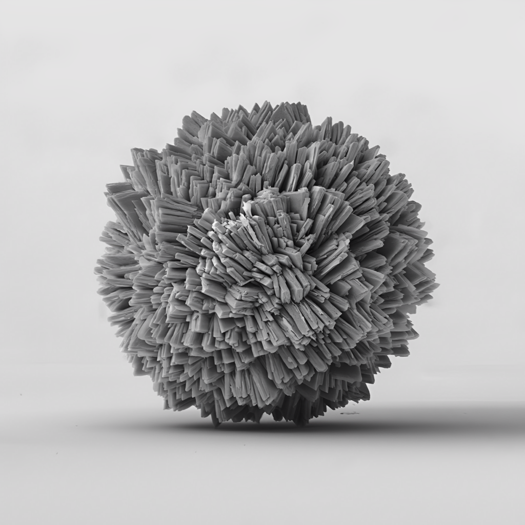
Reversible self-assembly of small molecules yielding tunable structures with multi-scale chirality is challenging, as the delicate balance of attraction-repulsion forces between chiral building blocks is hard to control. The microparticles captured here are made of copper-amino acid complex gradually forming chiral nanoclusters, polymerizing into two-dimensional, atomically thin nanosheets, which eventually self-assemble into spiky particles. The morphology and chiroptical properties of these particles can be controlled by various stimuli, such as temperature, light, pH or enantiomeric excess. Furthermore, they can be reversibly disassembled into primary building blocks and “on demand” reassembled into other suprastructures of complex symmetry. This facilitates their application in trapping, release and separation of enantiomers and optically active biocomponents, as well as in catalysis – analogously to copper metalloenzymes.
“Superchiral Particles” included a series of images. Others are shared below for further context.


Runner-Up, SEM
Catherine Haslam, “Finding Love in Lithium,” acquired on the TESCAN MIRA3
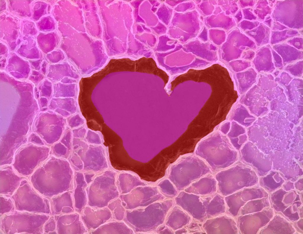
This image shows the surface of a solid-state electrolyte with in-situ plated lithium metal. The current collector was removed to image the surface, causing ductile failure of the lithium metal and a typical cup and cone fracture morphology, plus an area that looked like a heart.
Best TEM
Suk Hyun Sung, “Stella,” acquired on the Thermo Fisher Talos F200X G2
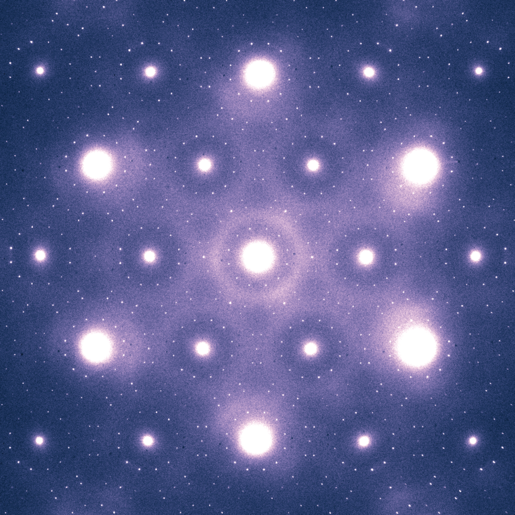
Selected Area Electron Diffraction (SAED) is a rudimentary but powerful technique that captures symmetries and symmetry breaking of crystalline specimens. Here, SAED pattern of TaS2 polytype heterostructure reveals three co-existing symmetry breaking: two mirror symmetric ‘ɑ’ and ‘β’ CDWs (charge density waves) and additional chemical ordering.
Runner-Up, TEM
Arkajit Ghosh and Bibhu Sahu, “Stair of Nano-Twins,” acquired on the Thermo Fisher Talos F200X G2
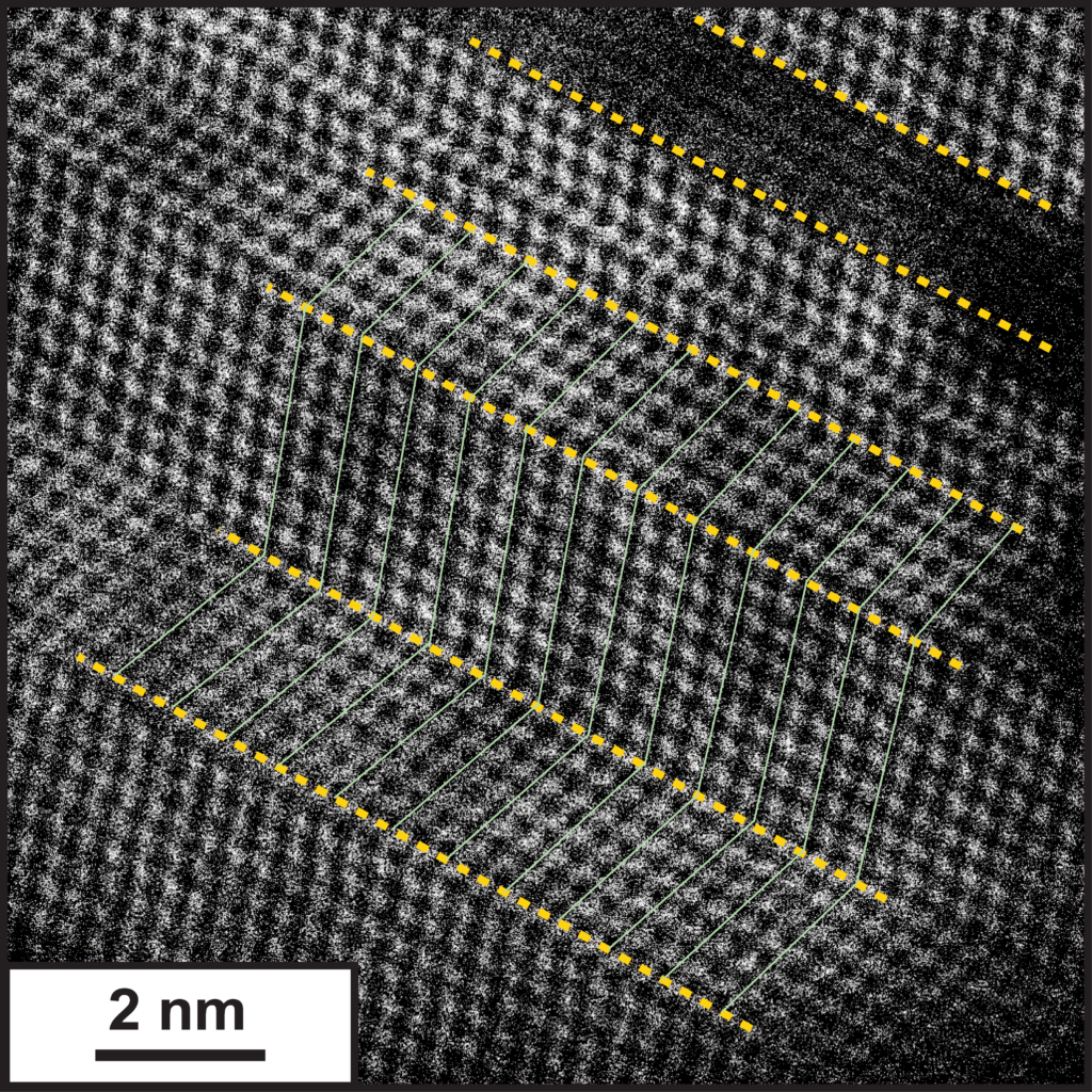
Atomic resolution nano-twins in Silicon fibers within laser surface remelted Al-Si nano eutectics. Highlighted the twin boundaries (dashed-yellow lines) and alternate atomic planes (green lines) for clear understanding.
Best Non-Electron Image
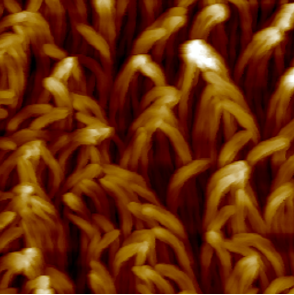
Xiaoyang Zhong and Arit Patra, “Nano-Scale Straw,” acquired on the Veeco Dimension Icon AFM
We used AFM to demonstrate polymer nanofibers fabricated by liquid crystal templated chemical vapor deposition polymerization.
Runner-Up, Non-Electron Image
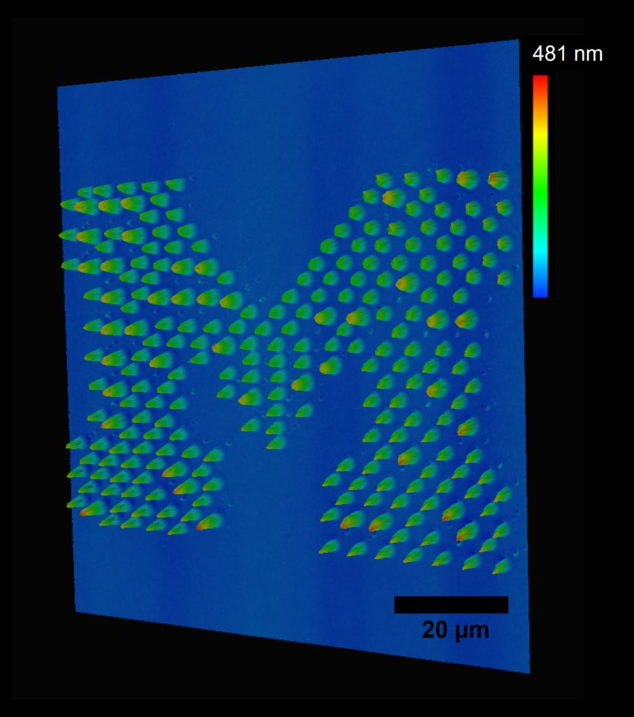
Brian Iezzi, “A Michigan Perspective,” acquired on the Veeco Dimension Icon AFM
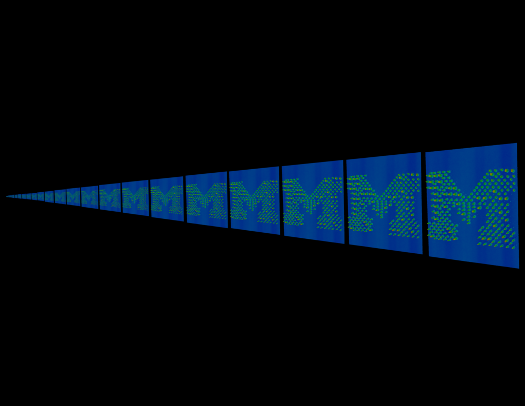
Electrohydrodynamic jet (e-jet) printing is a high resolution (<100 nm) micro/nano additive manufacturing method. This image shows a perspective array of atomic force microscope scans of e-jet printed germanium microarrays in block M arrangement for use in customized infrared photonic applications.
The original AFM scan is shown below.
