
Congratulations to the winners of the first (MC)2 image contest!
1st Place, Wonjin Choi, “Dandelion Pollen Grain” (Image acquired from the Tescan MIRA3 SEM)
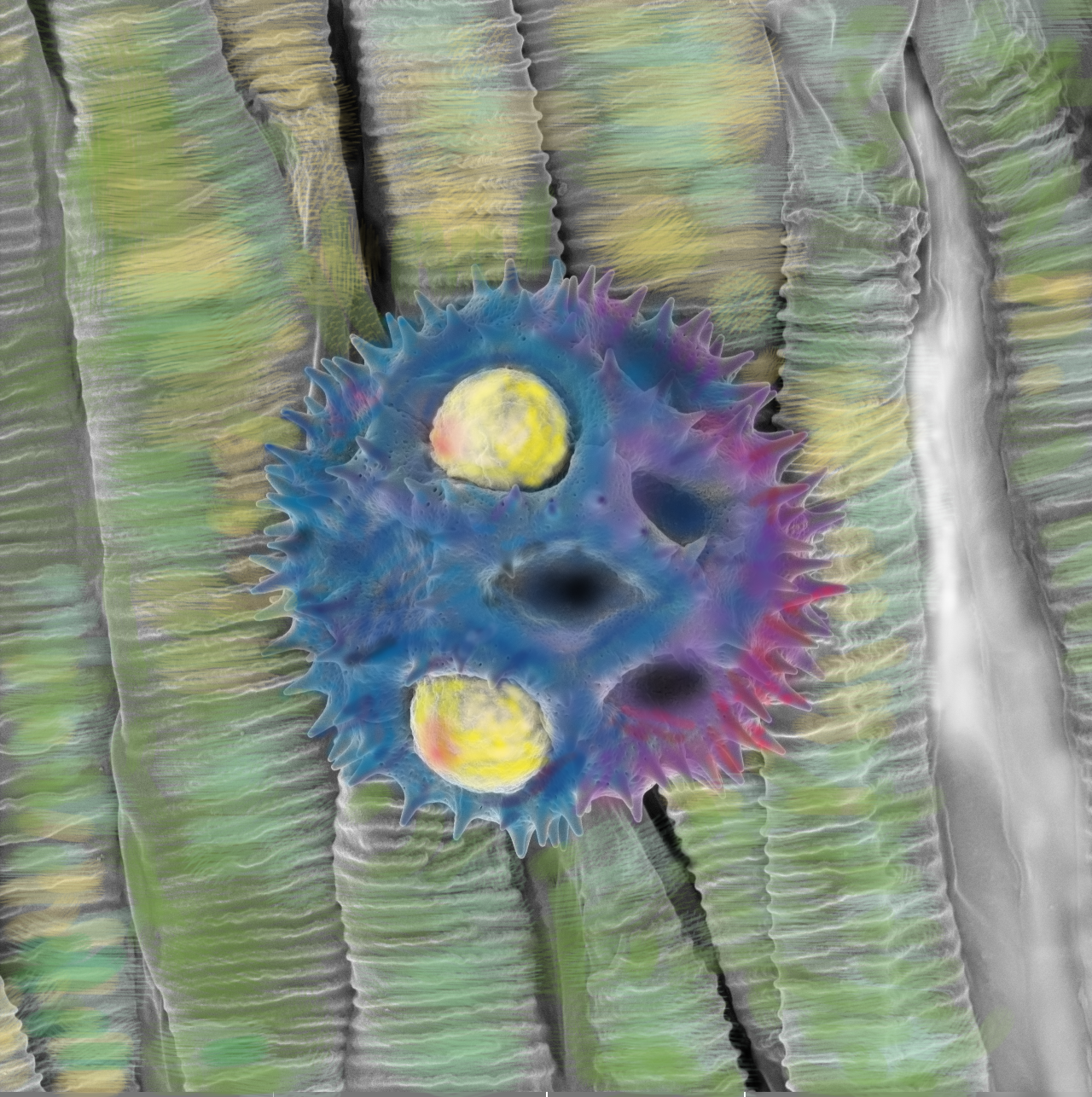
“This image is an SEM image of a dandelion pollen grain, a reproductive micro structure produced by the male part of a plant. Spiky surfaces can help them to cling to the carrier and transport the grains. The diameter of pollen is about 20 microns. False colors are used to create a mysterious atmosphere.”
Runners-up:
Suk Hyun Sung, “Sub-angstrom resolution, picometer precision characterization of charge density wave material system 1T-TaSSe” (Image acquired from the JEOL 3100R05 TEM)
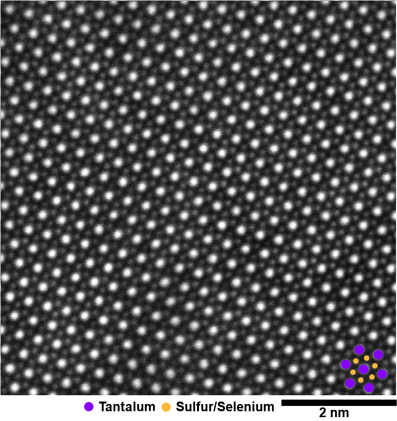
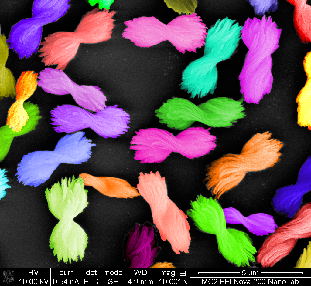
“Layered material 1T-TaSxSe1-x exhibits extraordinary phase transition (including metal-insulator transition, and super-conductivity) thanks to charge density wave and associated periodic lattice distortion. To characterize the phenomena, sub-Angstrom and picometer precision is essential. Here, the HAADF-STEM image taken on JEOL 3100 R05 demonstrates 80 pm resolution with sub 10 pm precision. The ‘Z’-contrast highlights heavy Tantalum atomic columns as well as Selenium rich columns. The image was averaged over 25 cross-correlated images.”Jiao Yan and Zhengzhi Mu, “Helical Candies – Trick or Treat” (Image acquired from the Nova SEM/FIB)
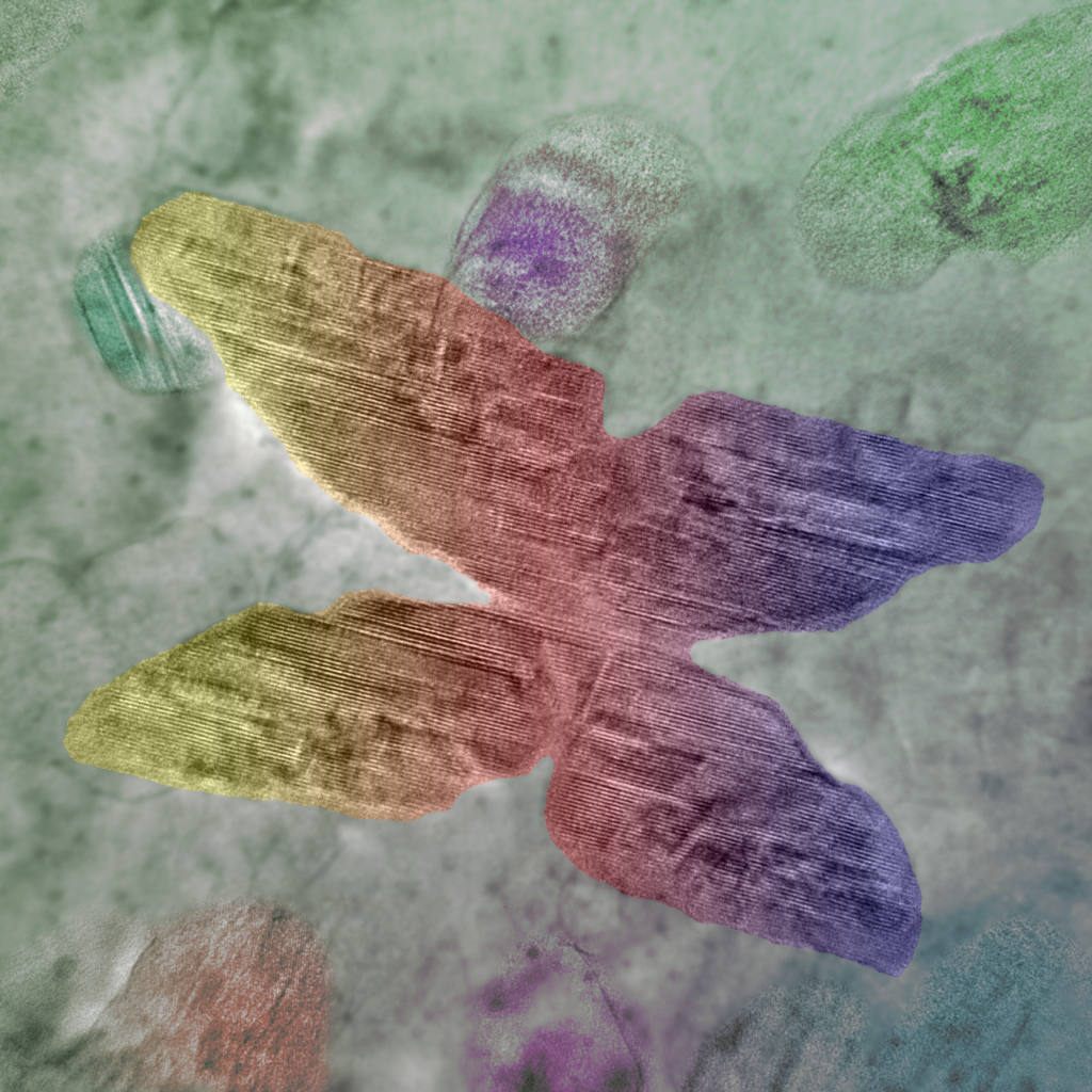
“Our group has been working on the fabrication of chiral materials for decades, and the helix is the most intuitive chiral structure. However, helical structures are not that easy to obtain considering its complexity. In this work, very uniform and clean helices with homochirality (right-handed) were fabricated. The helices look very much like candies, and they were taken around Halloween, so we colored all the helices in the image with different colors.”Huai-Hsun Lien, “The butterfly ‘D’ effect” (Image acquired from the JEOL 2010F TEM)
“This image is taken in Al-20 wt.% Si sample that is laser treated, the high cooling rate results in ultrafine Si grains as shown in the image. Each of the ‘butterfly’ wings spans 50 nm in width and 100 nm in length, which is unattainable in conventional casting techniques. The significance of the defects will manifest themselves in mechanical response. False colors are used and some blurring of the image to highlight the ‘butterfly’ structure.”